Nand Gate Schematic In Cadence
Xnor nand vdd Nand cadence virtuoso fig48 Cadence virtuoso:: layout of nand gate || part-2.
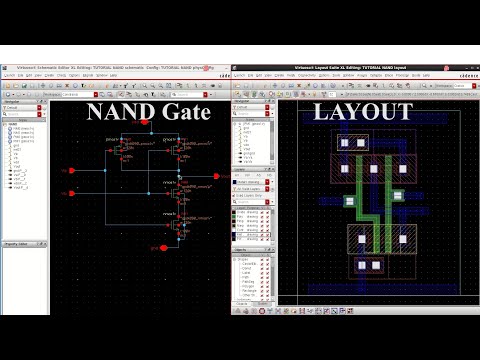
1: A 2-input NAND gate layout designed in Cadence Virtuoso. | Download
Nand cadence virtuoso gate lvs layout stack problems vlsi schematic integrated circuit Nand finfet 7nm geometries 9nm respectively Cadence tutorial -cmos nand gate schematic, layout design and physical
Cadence nand gate virtuoso using simulation
Cadence schematic gate layout nand cmos assura verificationLayout nand virtuoso gate cadence Layout of nand gate using cadence virtuoso toolCadence virtuoso tutorial: cmos nand gate schematic symbol and layout.
Lab 03 cmos inverter and nand gates with cadence schematic composerSolved problem 1 assignment is to create an xnor gate Lab 03 cmos inverter and nand gates with cadence schematic composer1: a 2-input nand gate layout designed in cadence virtuoso..

Nand layout cadence virtuoso gate tool using
Layout geometries of 7nm finfet nand gates with l g =7nm and 9nmNand cadence virtuoso cmos Inverter nand cadence nmos pmos cmos multiplierVirtuoso tutorial cadence layout inverter nand gate cmos pdf basic software line.
Cadence tutorialSimulation of basic nand gate using cadence virtuoso tool Integrated circuitCadence inverter composer schematic cmos nand pmos nmos tutorial.


Lab 03 CMOS Inverter and NAND Gates with Cadence Schematic Composer

integrated circuit - NAND gate LVS problems in Cadence Virtuoso
Cadence Virtuoso:: Layout of NAND Gate || Part-2. - YouTube

Cadence tutorial - Layout of CMOS NAND gate - YouTube

Cadence tutorial -CMOS NAND gate schematic, layout design and Physical

Layout of NAND Gate using Cadence Virtuoso Tool - YouTube

Solved Problem 1 Assignment is to create an XNOR gate | Chegg.com

Layout geometries of 7nm FinFET NAND gates with L G =7nm and 9nm

1: A 2-input NAND gate layout designed in Cadence Virtuoso. | Download

Lab 03 CMOS Inverter and NAND Gates with Cadence Schematic Composer